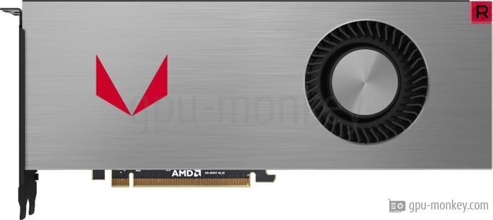
Sapphire Radeon RX Vega 64 LE
vs
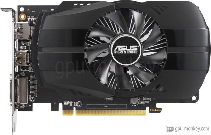
ASUS Phoenix Radeon RX 550 2G EVO
GPU comparison with benchmarksThe Sapphire Radeon RX Vega 64 LE has 4096 shader units and these clock a maximum of 1.55 GHz which results in an FP32 computing power of 12.66 TFLOPS.
The ASUS Phoenix Radeon RX 550 2G EVO has 512 shader units and these clock at a maximum of 1.18 GHz and achieve an FP32 computing power of 1.21 TFLOPS. |
||
GPUThe Sapphire Radeon RX Vega 64 LE is equipped with a graphics chip of the GCN 5 architecture, which has 64 streaming multiprocessors. The graphics card ASUS Phoenix Radeon RX 550 2G EVO is based on the GCN 4 architecture and is equipped with 8 execution units. |
||
| Sapphire Radeon RX Vega 64 LE | GPU | ASUS Phoenix Radeon RX 550 2G EVO |
| AMD RX Vega 64 | Based on | AMD Radeon RX 550 (Lexa) |
| Vega 10 XT | GPU Chip | Lexa PRO |
| GCN 5 | Architecture | GCN 4 |
| 64 | Streaming Multiprocessors | 8 |
| 4096 | Shader | 512 |
| 64 | Render Output Units | 16 |
| 256 | Texture Units | 32 |
| 0 | Raytracing Cores | 0 |
MemoryThe Sapphire Radeon RX Vega 64 LE is equipped with a 8 GB large HBM2 graphics memory, which is equipped with 0.945 GHz clocks. The ASUS Phoenix Radeon RX 550 2G EVO has a 2 GB large GDDR5 graphics memory and the memory clock is 1.500GHz. |
||
| 8 GB | Memory Size | 2 GB |
| HBM2 | Memory Type | GDDR5 |
| 0.945 GHz | Memory Clock | 1.500 GHz |
| 1.9 Gbps | Memory Speed | 6.0 Gbps |
| 484 GB/s | Memory bandwidth | 96 GB/s |
| 2048 bit | Memory Interface | 128 bit |
Clock SpeedsThe Sapphire Radeon RX Vega 64 LE has a turbo clock of 1.546 GHz. The turbo frequency of the ASUS Phoenix Radeon RX 550 2G EVO is 1.183 GHz. |
||
| 1.247 GHz | Base Clock | 1.100 GHz |
| 1.546 GHz | Boost Clock | 1.183 GHz |
| Avg (Game) Clock | ||
| Yes | Overclocking | Yes |
Thermal DesignThe Sapphire Radeon RX Vega 64 LE has 2 x 8-Pin connectors through which it is supplied with power. The manufacturer specifies the maximum operating temperature of the graphics card as 100 °C. The ASUS Phoenix Radeon RX 550 2G EVO is equipped with a PCIe power connector that supplies it with power. The maximum operating temperature of the card is 80 °C. |
||
| 295 W | TDP | 50 W |
| -- | TDP (up) | -- |
| 100 °C | Tjunction max | 80 °C |
| 2 x 8-Pin | PCIe-Power | |
Cooler & FansThe graphics processor and graphics memory of the Sapphire Radeon RX Vega 64 LE are cooled with a Air cooling. The ASUS Phoenix Radeon RX 550 2G EVO is cooled by a Air cooling. |
||
| Radial | Fan-Type | Axial |
| 1 x 75 mm | Fan 1 | 1 x 80 mm |
| -- | Fan 2 | -- |
| Air cooling | Cooler-Type | Air cooling |
| dB | Noise (Idle) | dB |
| -- | Noise (Load) | -- |
ConnectivityThe Sapphire Radeon RX Vega 64 LE supports the downward compatible copy protection HDCP in version 2.2. The ASUS Phoenix Radeon RX 550 2G EVO supports HDCP in version 2.2 and all previous versions. |
||
| 4 | Max. Displays | 4 |
| 2.2 | HDCP-Version | 2.2 |
| 1x HDMI v2.0b | HDMI Ports | 1x HDMI v2.0b |
| 3x DP v1.4 | DP Ports | 1x DP v1.4 |
| -- | DVI Ports | 1 |
| -- | VGA Ports | -- |
| -- | USB-C Ports | -- |
FeaturesetThe Sapphire Radeon RX Vega 64 LE supports the DirectX standard from Microsoft in version 12_1. The ASUS Phoenix Radeon RX 550 2G EVO supports Microsoft's DirectX version 12. |
||
| 7680x4320 | Max. resolution | 5120x2880 |
| 12_1 | DirectX | 12 |
| No | Raytracing | No |
| Yes | DLSS / FSR | Yes |
| Non addressable LED | LED | No LED lighting |
Supported Video CodecsThis area lists which video codecs can be decoded or encoded by the graphics cards in hardware. As a result, the power consumption can be reduced due to a lower processor load. |
||
| Decode / Encode | h264 | Decode / Encode |
| Decode / Encode | h265 / HEVC | Decode / Encode |
| No | AV1 | No |
| Decode | VP8 | Decode |
| Decode / Encode | VP9 | Decode |
DimensionsThe Sapphire Radeon RX Vega 64 LE is 40 mm wide and therefore needs the space of 2 PCIe-Slots in the case. The width of the ASUS Phoenix Radeon RX 550 2G EVO is 40 mm and thus requires the space of 2 PCIe-Slots in the PC case. |
||
| 282 mm | Length | 192 mm |
| 125 mm | Height | 115 mm |
| 40 mm | Width | 39 mm |
| 2 PCIe-Slots | Width (Slots) | 2 PCIe-Slots |
| -- | Weight | -- |
| PCIe 3.0 x 16 | GPU Interface | PCIe 3.0 x 8 |
| No | SFF-Ready | No |
Additional dataManufactured using the 14 nanometer process, Sapphire Radeon RX Vega 64 LE was released in Q3/2017. The ASUS Phoenix Radeon RX 550 2G EVO published in Q2/2017 is manufactured with a structure width of 14 nanometers. |
||
| 21275-01 | Part-no | PH-RX550-2G-EVO |
| Q3/2017 | Release date | Q2/2017 |
| 499 $ (Reference) | Launch Price | 79 $ (Reference) |
| 14 nm | Structure size | 14 nm |
| data sheet | Documents | data sheet |
1.247 GHz, 8 GB (295 W TDP)
Buy this graphic card at amazon!
1.100 GHz, 2 GB (50 W TDP)
Buy this graphic card at amazon!
Rate these graphics cards now
Benchmark results
3DMark Benchmark (DirectX, Raytracing)
3DMark is a benchmark program that determines the performance of certain components of a computer and then reports the performance as a numerical value.
Time Spy Extreme Graphics score

|
Sapphire Radeon RX Vega 64 LE
8 GB HBM2 |
||

|
ASUS Phoenix Radeon RX 550 2G EVO
2 GB GDDR5 |
||
Battlefield 5
Battlefield 5 is a visually stunning game that is ideal as a graphics card benchmark. We test the game with maximum details on Windows 10.
3840x2160 (2160p)
|
|
Sapphire Radeon RX Vega 64 LE
8 GB HBM2 |
||
|
|
ASUS Phoenix Radeon RX 550 2G EVO
2 GB GDDR5 |
||
2560x1440 (1440p)
|
|
Sapphire Radeon RX Vega 64 LE
8 GB HBM2 |
||
|
|
ASUS Phoenix Radeon RX 550 2G EVO
2 GB GDDR5 |
||
1920x1080 (1080p)
|
|
Sapphire Radeon RX Vega 64 LE
8 GB HBM2 |
||
|
|
ASUS Phoenix Radeon RX 550 2G EVO
2 GB GDDR5 |
||
Geekbench 6 (OpenCL, Vulkan, Metal)
Geekbench 6 is a cross-platform benchmark for main processors, which also carries out 3 different graphics benchmarks and outputs them in the form of a numerical value.
Geekbench 6 - OpenCL
|
|
Sapphire Radeon RX Vega 64 LE
8 GB HBM2 |
||
|
|
ASUS Phoenix Radeon RX 550 2G EVO
2 GB GDDR5 |
||
Geekbench 6 - Vulkan
|
|
Sapphire Radeon RX Vega 64 LE
8 GB HBM2 |
||
|
|
ASUS Phoenix Radeon RX 550 2G EVO
2 GB GDDR5 |
||
Geekbench 6 - Metal
|
|
Sapphire Radeon RX Vega 64 LE
8 GB HBM2 |
||
|
|
ASUS Phoenix Radeon RX 550 2G EVO
2 GB GDDR5 |
||
FP32 Performance (Single-precision TFLOPS)
The theoretical computing power of the graphics card with single precision (32 bit) in TFLOPS indicates how many trillion FP32 floating point operations the graphics card (GPU) can perform per second.
FP32 (TFLOPS)
|
|
Sapphire Radeon RX Vega 64 LE
8 GB HBM2 |
||
|
|
ASUS Phoenix Radeon RX 550 2G EVO
2 GB GDDR5 |
||


